Synopsys joins Intel’s chip design services program
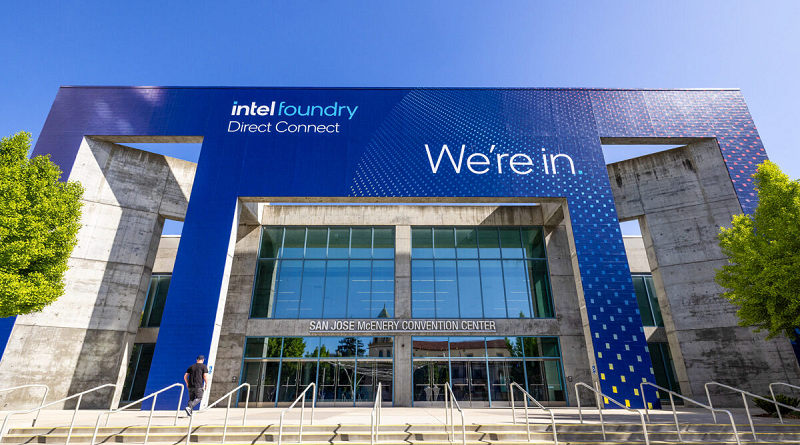
Every year, Intel hosts an event called Direct Connect where it previews upcoming upgrades to its chip factories. The tech industry pays attention because those factory upgrades determine how much faster processors will get in the subsequent quarters. This year’s event saw Intel demonstrate several new technologies, including one that can combine multiple chips into a single processor by stacking them atop one another.
The other focus of the event, which took place on April 29, was Intel’s partner ecosystem. Synopsys, one of the world’s top providers of chip design software, announced that it has joined Intel’s Design Services Alliance. This is a program through which firms working on custom chips can access semiconductor design consulting services. The partner-related announcements at Intel’s event also included new technology reveals from Cadence Design Systems, Keysight and Siemens, three of Synopsys’ largest competitors.
Hiring a chip consultant
For about half a century, Intel used its factories almost solely to produce internally-designed chips. A few years ago, the company started shifting to a so-called foundry business model. Intel’s factories can now make chips for other firms based on designs supplied by those firms. This is where the Design Services Alliance that Synopsys has joined comes into the picture.
The kind of company that signs a deal with a foundry to mass produce a custom processor has plenty of in-house chip expertise. However, semiconductor projects are so complicated that even the most tech-savvy firm can run into obstacles. A startup developing a new smartwatch chip might have limited experience designing circuits that can run AI models efficiently. A big cloud provider, meanwhile, may need help building out its newest server chip’s security coprocessor. When such situations emerge, companies hire a chip design consultancy to fill their knowledge gaps. Firms that partner with Intel to make their chips can access chip design consultancies’ know-how through the Design Services Alliance. Synopsys is one of a dozen companies that are providing their expertise through the program.
“This exciting collaboration with Synopsys, which will bring key EDA design flows and IP to Intel 18 and Intel 18A-P, both demonstrates and reinforces the strong momentum of the Intel Foundry ecosystem,” Suk Lee, the vice president and general manager of Intel’s Ecosystem Technology Office, told Boardroom Insight. “We are pleased to collaborate with Synopsys to provide our customers with the critical capabilities to meet the demands of the AI era.”
When we reached out to Synopsys for more information, a spokesperson shared a marketing page that outlined the consulting services available through Intel’s Design Services Alliance. The process of creating a custom processor design is only one of the tasks that those consulting services promise to ease. Synopsys can also help customers with the project management aspect of chip development initiatives. Additionally, the company provides so-called post-silicon services. This means it can help clients optimize a chip project once production has already begun, for example by troubleshooting manufacturing defects.
EDA flows are another focus of Synopsys’ professional services business. “An EDA flow is the sequence of well-defined and validated steps to design and manufacture a chip,” a Synopsys spokesperson explained. “Synopsys’ qualified EDA flows and design IP can help designers and foundries mitigate manufacturing challenges – helping mutual customers design and manufacture with increased confidence and improved quality and time to market.”
Companies can also hire Synopsys to improve their own internally-developed EDA flows. A firm might, for example, wish to speed up the workflow through which it develops car chips by deploying an AI tool to automate repetitive tasks. Synopsys also offers pre-optimized flows that remove the need for clients to develop an entire chip design methodology from scratch.
Alongside the news that it’s joining Intel’s chip consulting program, Synopsys announced an update to its catalog of ready-made chip design flows. The company revealed that several of its AI-powered flows for designing digital and analog chips will work with Intel 18A, Intel’s next flagship manufacturing process.
The flows “are certified by Intel Foundry for the Intel 18A technology node, helping mutual customers to manufacture with confidence on that node,” the Synopsys spokesperson added.
The company is also rolling out flows for Intel 18A-P, a version of the manufacturing process designed to provide more computing power. Intel is promising 8% higher performance per watt compared with the standard variant.
“The value the announced Synopsys / Intel Foundry collaboration adds is that it makes Intel 18A more attractive by providing ready-made EDA flows and industry-standard IP that customers can use without needing to duplicate effort and create these capabilities independently,” an Intel spokesperson told Boardroom Insight.
Besides EDA flows and consulting services, Intel customers who need help with their chip projects also have access to other resources. Those other resources include a so-called process design kit, or PDK, that can help semiconductor engineers more quickly get started with Intel 18A. “In the same way that SDKs give developers access to the ‘building blocks’ they need to create software for a given platform, a PDK provides designers with the specs they need for a particular chip manufacturing process,” the Intel spokesperson explained.
The broader EDA ecosystem
Synopsys’ top rivals were also present at the Intel event where the EDA provider updated its chip design flow lineup. Cadence, Keysight and Siemens introduced new offerings that will help customers make processors using Intel 18A. Like Synopsys, the three firms sell EDA software that engineers use to speed up chip development.
Cadence says that its RTL-to-GDS chip design flow has been certified for the Intel 18A process development kit. At the start of a chip project, engineers define the high-level details of a new processor using a technology called RTL. Once the chip blueprint is ready at the end of the project, the design is saved in a format called GDS that can be sent to the manufacturer. Cadence’s RTL-to-GDS flow is powered by more than ten of the company’s chip development applications.
Keysight, in turn, revealed an update to its competing EDA software that adds support for Intel’s newly announced EMIB-T technology. EMIB-T allows engineers to integrate multiple chips into one large processor. The technology works by placing the chips that need to be integrated on a substrate, which is a flat panel that functions as a support structure. Components called bridges that are embedded in the substrate allow data to flow between the chips. Data travels through the bridges via wires known as through-silicon vias.
EMIB-T is an upgraded version of a technology called EMIB that Intel first unveiled in 2017. EMIB didn’t include through-silicon vias. According to Intel, the addition of the wires will make it easier to port processor designs to EMIB-T from competing chip interconnect technologies.
EMIB-T and Intel 18A were also a major focus of Siemens’ product updates at Direct Connect. The company has released a reference EDA flow that will make it easier for chip designers to use EMIB-T. Additionally, it has certified its Solido SPICE, Analog FastSPICE and Calibre nmPlatform applications for the Intel 18A PDK. The former two applications can test a newly developed chip design in simulations to uncover any errors that engineers may have overlooked. Calibre nmPlatform, in turn, speeds up the sign-off phase of semiconductor projects, which likewise focuses on resolving design issues before a processor enters mass production.
The road ahead
Intel expects to move Intel 18A into volume production by the end of the year. If everything goes according to plan, the process will be followed by an even more capable manufacturing technology called Intel 14A in 2027. Cadence has already started optimizing its EDA flows for the upcoming process, in particular a variant called Intel 14A-E that is expected to provide an expanded set of features.
A chip’s clock frequency, a property that directly influences performance, is bottlenecked by components called critical paths. The higher the frequency of a processor’s critical paths, the higher the frequency of the processor. Intel 14A includes a technology called Super Cells that will make it easier for chip designers to optimize critical paths and thereby boost processor performance.
Intel 18A is set to provide up to 25% better performance per watt than the newest process that the company is currently using for mass production. Intel 14A, in turn, is expected to offer 20% higher performance per watt than Intel 18A. Engineers working on power-constrained chips can optionally swap some of that extra speed for lower electricity use. By Intel’s estimates, Intel 14A will be capable of providing the same compute capacity as Intel 18A with 35% lower electricity consumption.
Photo courtesy of Intel


text
text